
What the company actually publishes
Based in Taiwan, MetaRosetta describes metalens design and product integration using semiconductor processes. Its customization page emphasizes computational optical design and delivery of design IP and process parameters for customers working with their own manufacturing partners. That is a different proposition from buying a fully qualified camera module.
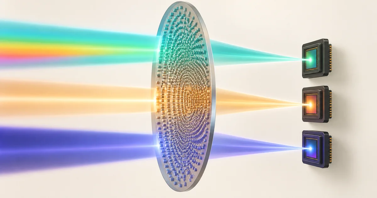
A metalens uses subwavelength structures to shape incoming light. The potential attraction is a thinner optical path or a function that would otherwise need several optical elements. The engineering test remains system performance: image quality, usable field of view, efficiency, manufacturability and cost in the target product. A 2026 technical review identifies trade-offs among these measures across metalens designs.
Three routes, three different starting points
Visible light
MetaRosetta describes a metasurface colour splitter for compact CMOS image sensors, directing light toward selected pixels. This is a pixel-level light-management concept; it should not be treated as evidence that a whole camera lens stack can be replaced.
Official visible-light page ↗Near infrared
The company positions a metalens as receiving optics for facial recognition and eye tracking in the 850–1550 nm range. The design question is whether the target wavelength, detector, illumination, working distance and field of view work together in a smaller module.
Official NIR page ↗Long-wave infrared
For 8–12 µm thermal imaging, MetaRosetta discusses industrial, vehicle and aerial applications. That makes size and weight worth investigating, while real performance still depends on the detector, housing, temperature range and optical test results.
Official LWIR page ↗Where a Canadian product team could start
Choose one narrow sensing task first: for example, a fixed-wavelength NIR receiver with a strict module-height limit, or a thermal camera whose optics dominate size and payload. Compare a conventional reference module and a proposed metasurface design under the same conditions. A thinner element only creates product value if the complete assembly meets the image, environmental and commercial requirements.
For an initial evaluation, request the following before a design commitment:
- Optical data: target wavelength or bandwidth, aperture, field of view, transmission or focusing efficiency definition, distortion, stray light and measured images at the intended operating points.
- System data: compatible detector and illumination, module stack height, alignment tolerance, packaging, thermal behaviour and environmental test conditions.
- Production data: sample availability, process flow, wafer-level yield evidence, repeatability, IP deliverables, manufacturing ownership, lead time and lifecycle plan.
The company's public pages describe intended applications and design capabilities. They do not, by themselves, establish a specific module's certification, production yield, Canadian availability or commercial terms. Those points need direct supplier evidence for the exact design.
FlyPig AI interpretationMetaRosetta is most useful to investigate when optics constrain the product architecture. Begin with a measured baseline and one target use case; assess the claimed thickness benefit against the whole sensor system, not the lens element alone.